
- aPeter Grünberg Institute PGI-5, Forschungszentrum Jülich, D-52425 Jülich, Germany
Originally published: 2012-03-02 in J. Appl. Phys. 111, 056101 (2012)
Gated variable resistors were manufactured by depositing epitaxial heterostructures of doped $\ce{La2CuO_{4+$\delta$}}$ and $\ce{SrTiO3}$ layers. Their conductance change as function of write current $I$ and write time $t$ followed a simple empirical law of the form $\Delta G/G = C I^A t^B$. This behavior is in agreement with ionic transport that accelerates exponentially with electrical field strength.
© (2012) American Institute of Physics. This article may be downloaded for personal use only. Any other use requires prior permission of the author and the American Institute of Physics.
The following article appeared in J. Appl. Phys. 111, 056101 (2012) and may be found at http://dx.doi.org/10.1063/1.3691599
Solid-state ionic transport on the nanoscale has recently attracted attention because it is believed to be crucial for the operation of two possible alternative concepts for computer memory: electrochemical metallization cells and devices based on local valence change of the cations through anion migration. [1] Although the applied voltages are only moderate, there are strong electrical fields present that accelerate the ionic transport exponentially by contributing part of the activation energy for ionic transport [2,3,4] . This contrasts with conventional ionic transport where the activation energy is solely provided by thermal excitation. Measuring the ionic transport in nanometer-thick films can be challenging, especially in the case of oxygen.

Figure 1: Sample structure from top to bottom. (I) silver contact pads; (II) passivation; (III) channel; (IV) channel contacts; (V) dielectric and ionic conductor; (VI) gate; (VII) substrate. The junction area is about 0.5 mm²
| Part | Material | d/nm | Doping |
|---|---|---|---|
| Gate | $\ce{La_{1.85}Sr_{0.15}CuO_{4+\delta}}$ | 20 | p |
| Dielectric | $\ce{SrTiO3}$ | 25 | intrinsic |
| Channel contacts | $\ce{La_{1.85}Sr_{0.15}CuO_{4+\delta}}$ | 20 | p |
| Channel | $\ce{La2CuO_{4+\delta}}$ | 5 | p |
| Passivation | $\ce{SrTiO3}$ | 10 | intrinsic |
We created a device to measure the change of in-plane conductance caused by the doping effect of out-of-plane oxygen anion transport similar to one reported by Ramesham et al.[5] . Epitaxial oxide structures were deposited through titanium shadow masks with high-pressure pure oxygen sputtering at 800 °C (heater temperature) on epi-polished single-crystal $\ce{SrTiO3}$ (100)K substrates from CrysTec (Berlin). A sketch of the different layers is shown in Figure 1 and the materials and thicknesses are given in Table 1. A sputtered silver layer of 600 nm thickness was used for the electrical connections to the oxide films.
For each layer, the chamber was first pumped down to a background pressure of less than $1\times10^{-5}$ mbar. Then the sample was heated to the deposition temperature in an atmosphere of 0.5 mbar oxygen within 45 minutes. Afterwards the sputter target was pre-sputtered for one hour, followed by layer deposition lasting from 30 minutes to 3 hours, depending on deposition rate and desired film thickness. The sample was finally cooled down in an atmosphere of 0.5 mbar oxygen.
The deposition rate was determined by measuring the thickness of the device structures with a profilometer after a very long deposition time to achieve sufficient film thickness and by examining cross-sections with SEM and TEM. The layer thickness is not uniform over the device area due to the shadowing effect of the masks that leads to very shallow slopes on the edges. The given thicknesses are therefore to be understood as approximate peak values in the middle of the structures.
$\ce{La2CuO_{4+\delta}}$ was chosen as the channel material because excess oxygen intercalates easily into the crystal structure even at room temperature and changes the material's behavior from semiconducting to metallic at sufficient concentration.[6]
Electrical properties were measured with a Keithley 6221 AC and DC current source, coupled with a Keithley 2182A nanovoltmeter. The positive current direction through the dielectric is defined as from the channel to the gate.

Figure 2: Current-voltage curve of the dielectric. Points: measurement; solid lines: fit with the indicated parameters for Eq. \eqref{eq:I_el}
The electronic current $I_{el}$ through the dielectric as a function of voltage $U$ can be described by the equation \begin{equation} I_{el} = I_{0,el} \left( \exp \left( a_{el} \times U \right) - 1 \right) \label{eq:I_el} \end{equation} with fit parameters $I_{0, el}, a_{el}$ being different for the positive and negative direction (Figure 2). This equation corresponds to the Shockley equation that describes the behavior of a diode. Yajima et al.[7] obtained comparable results with Al/$\ce{SrTiO3}$/$\ce{La_{0.7}Sr_{0.3}MnO3 }$/Nb:$\ce{SrTiO3}$ heterojunctions. Hikita et al. [8] also reported that the barrier height of $\ce{La_{0.7}Sr_{0.3}MnO3 }$/Nb:$\ce{SrTiO3}$ depends sensitively on the surface termination of the interface. This strong influence of termination could explain the spread of one order of magnitude in dielectric properties observed by us between two devices manufactured in one process on the same substrate.
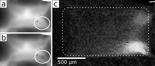
Figure 3: Reversible changes visible in an optical microscope (reflected light) after writing for 10 minutes with +20 mA. (a) and (b) show the sample before and after writing, respectively, while (c) is the difference of the two images. The dotted line in (c) outlines the crossing area between channel and gate (compare Figure 1). The current flowed between the lower (channel) and the right (gate) side, and the change is localized in the area of maximum field strength in the dielectric.
The current-voltage characteristics of the dielectric could only be measured accurately under conditions where the voltage drop over channel and gate, forming the electrodes (resistance typically between 1 kΩ and 10 kΩ), was small compared to the voltage drop across the dielectric. Only under such conditions is the voltage drop across the dielectric nearly constant over the entire electrode area and can be measured in a four-point configuration using the two channel and gate electrodes. In other cases, the voltage also drops significantly inside the large-area electrodes, which distorts the measurements especially at higher currents, as the current through the dielectric grows exponentially with applied voltage, while the electrodes show ohmic behavior. This effect is responsible for the localized writing effect in Figure 3, where the visible change is concentrated in the corner with maximum voltage drop across the dielectric.

Figure 4: Conductance change during a writing experiment with increasing current. (a) shows the the absolute conductance values and write pulses over the course of the experiment, while in (b) the conductance change relative to the previous measured point is plotted as function of write time for positive write currents, along with a fit of Eq. \ref{eq:DG_G} ($C$=0.032, $A$=0.36, $B$=0.27) as solid lines. Data below 10 ms write time is omitted because of dominating noise and drift. The corresponding plot for negative currents would be similar. Legend (write current, minimum write time): (1) 13.8 µA, 38.6 ms; (2) 29.2 µA, 18.2 ms; (3) 61.2 µA, 8.55 ms; (4) 132 µA, 4.03 ms; (5) 280 µA, 1.89 ms; (6) 596 µA, 892 µs; (7) 1.27 mA, 420 µs; (8) 2.69 mA, 198 µs; (9) 5.71 mA, 93.0 µs; (10) 12.1 mA, 43.8 µs
In conclusion, we present a non-volatile variable resistor based on epitaxial oxide heterostructures. The resistance change as a function of write current and write time follows a simple empirical law over a wide range of currents and times. The time-domain behavior is similar to dielectric relaxation caused by slowly mobile charge carriers. The current dependence in connection with bubble formation can be interpreted as evidence for ionic transport that accelerates exponentially with increasing field strength and is very slow in absence of a field that contributes to the activation energy for transport. Exponential increase of write speed with voltage was observed perviously by Terabe et al. for variable metal filaments [11] and by Pickett et al. for tunneling contacts [12] . Measuring the conductance change of a doped semiconductor allows more direct conclusions on the amount of transported ions: The conductance change should be proportional to the change in carrier density and mobility and therefore proportional to the amount of transported ions in the range of small relative concentration changes. Our device can therefore be a valuable tool for studying low-level oxygen transport parallel to a large electronic current in nanometer-thick films under strong electrical fields over a wide parameter range. A gated variable resistor also has potential applications in reconfigurable logic circuits or artificial neuronal networks. [5,13,14,15]
Footnotes
References
- [1]
- Rainer Waser, Masakazu Aono: Nanoionics-based resistive switching memories. Nat. Mater. 6(11):833–840, November 2007. DOI: 10.1038/nmat2023. ↰
- [2]
- David R. Lamb: Electrical Conduction Mechanisms in Thin Insulating Films. pages 14–22, Methuen and Co, 1967. ↰ ↰
- [3]
- R. Meyer, L. Schloss, J. Brewer, R. Lambertson, W. Kinney, J. Sanchez, D. Rinerson: Oxide dual-layer memory element for scalable non-volatile cross-point memory technology. In Non-Volatile Memory Technology Symposium, 2008. NVMTS 2008. 9th Annual, pages 1 -5, 2008. DOI: 10.1109/NVMT.2008.4731194. ↰ ↰
- [4]
- Dmitri Strukov, R. Williams: Exponential ionic drift: fast switching and low volatility of thin-film memristors. Appl. Phys. A: Mater. Sci. Process. 94(3):515–519, March 2009. DOI: 10.1007/s00339-008-4975-3. ↰
- [5]
- R. Ramesham, S. Thakoor, T. Daud, A. P. Thakoor: Solid-State Reprogrammable Analog Resistive Devices for Electronic Neural Networks. J. Electrochem. Soc. 137(6):1935-1939, 1990. DOI: 10.1149/1.2086834. ↰ ↰ ↰
- [6]
- A. Daridon, H. Siegenthaler, F. Arrouy, E. J. Williams, E. Mächler, J. -P. Locquet: Growth and electrochemical oxidation of MBE-grown c-axis $\ce{La2CuO4}$ thin films on different substrates. J. Alloys Compd. 251(1-2):118 - 122, 1997. DOI: 10.1016/S0925-8388(96)02804-6. ↰
- [7]
- Takeaki Yajima, Yasuyuki Hikita, Harold Y. Hwang: A heteroepitaxial perovskite metal-base transistor. Nat. Mater. 10(3):198-201, Jan. 2011. DOI: 10.1038/nmat2946. ↰
- [8]
- Yasuyuki Hikita, Mitsuru Nishikawa, Takeaki Yajima, Harold Y. Hwang: Termination control of the interface dipole in $ \ce{La_{0.7}Sr_{0.3}MnO3}$/Nb:$\ce{SrTiO3}$ (001) Schottky junctions. Phys. Rev. B 79(7):073101, Feb. 2009. DOI: 10.1103/PhysRevB.79.073101. ↰
- [9]
- Andrew K Jonscher: Dielectric relaxation in solids. J. Phys. D: Appl. Phys. 32(14):R57, 1999. DOI: 10.1088/0022-3727/32/14/201. ↰
- [10]
- Chen Ang, Zhi Yu, L. E. Cross, Ruyan Guo, A. S. Bhalla: Dielectric relaxation and conduction in $\ce{SrTiO3}$ thin films under DC bias. Appl. Phys. Lett. 79(6):818-820, 2001. DOI: 10.1063/1.1389771. ↰
- [11]
- K. Terabe, T. Hasegawa, T. Nakayama, M. Aono: Quantized conductance atomic switch. Nature 433(7021):47–50, January 2005. DOI: 10.1038/nature03190. ↰
- [12]
- Matthew D. Pickett, Dmitri B. Strukov, Julien L. Borghetti, J. Joshua Yang, Gregory S. Snider, Duncan R. Stewart, R. Stanley Williams: Switching dynamics in titanium dioxide memristive devices. J. Appl. Phys. 106(7):074508, 2009. DOI: 10.1063/1.3236506. ↰
- [13]
- T. Sakamoto, N. Banno, N. Iguchi, H. Kawaura, S. Kaeriyama, M. Mizuno, K. Terabe, T. Hasegawa, M. Aono: Three terminal solid-electrolyte nanometer switch. In Electron Devices Meeting, 2005. IEDM Technical Digest. IEEE International, pages 475 -478, 2005. DOI: 10.1109/IEDM.2005.1609383. ↰
- [14]
- Toshitsugu Sakamoto, Noriyuki Iguchi, Masakazu Aono: Nonvolatile triode switch using electrochemical reaction in copper sulfide. Appl. Phys. Lett. 96(25):252104, 2010. DOI: 10.1063/1.3457861. ↰
- [15]
- Tsuyoshi Hasegawa, Yaomi Itoh, Hirofumi Tanaka, Takami Hino, Tohru Tsuruoka, Kazuya Terabe, Hisao Miyazaki, Kazuhito Tsukagoshi, Takuji Ogawa, Shu Yamaguchi, Masakazu Aono: Volatile/Nonvolatile Dual-Functional Atom Transistor. Appl. Phys. Express 4(1):015204, 2011. DOI: 10.1143/APEX.4.015204. ↰
Comments
Comments are closed.